Electroless Nickel Plating
化学镀镍
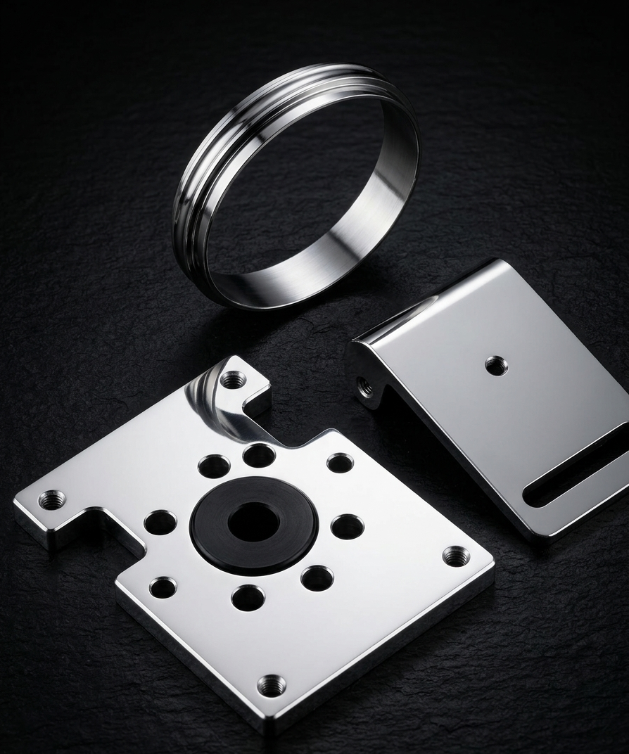
Chemical nickel plating delivering uniform thickness on complex geometries and high surface hardness.
Electroless Nickel (EN) plating is a chemical deposition process — unlike electroplating, it requires no electrical current and deposits a perfectly uniform nickel-phosphorus alloy layer regardless of part geometry. This makes it ideal for blind holes, internal bores, and complex 3D shapes that electroplating cannot coat uniformly.
At Active Treatment, we offer medium-phosphorus (6–9% P) and high-phosphorus (10–13% P) electroless nickel, each with different hardness and corrosion performance characteristics. The as-deposited hardness of ~HV 500 can be increased to ~HV 900 by heat treatment.
Our EN line serves the semiconductor equipment, oil & gas, and precision engineering sectors where dimensional accuracy and corrosion performance are non-negotiable.
Key Benefits
- Perfectly uniform thickness on any geometry
- As-deposited hardness HV 500, up to HV 900 after heat treatment
- Excellent corrosion resistance in acidic environments
- Good solderability and bondability
- RoHS compliant
Specifications
| Substrate | Steel, stainless steel, aluminium, copper alloys |
|---|---|
| Thickness | 5–50 µm |
| Phosphorus content | 6–9% (medium-P), 10–13% (high-P) |
| Post-heat hardness | HV 850–1000 |
| As-deposited hardness | HV 450–550 |
Frequently Asked Questions
What is the difference between medium and high phosphorus EN?
Medium-P (6–9%) EN has higher as-deposited hardness and better wear resistance. High-P (10–13%) EN has lower crystallinity (near-amorphous), offering superior corrosion resistance in aggressive chemical environments. Choose high-P for chemical or marine exposure, medium-P for wear applications.
Can electroless nickel be plated on aluminium?
Yes. Aluminium requires a zincate pre-treatment before EN plating to ensure adhesion. We perform this in-house. Please specify the alloy so we can select the appropriate pre-treatment.
What does heat treatment do to electroless nickel?
Heat treatment at 350–400°C converts the amorphous nickel-phosphorus deposit to a crystalline Ni3P structure, increasing hardness from ~HV 500 to ~HV 900. This also improves adhesion but slightly reduces corrosion resistance.
Is electroless nickel suitable for semiconductor components?
Yes. Our cleanroom-adjacent EN line meets the purity requirements of the semiconductor sector. We plate wafer handling arms, vacuum chucks, and precision jigs regularly.
How do I specify the EN thickness for my application?
Typical engineering applications use 12–25 µm. Wear-critical applications may specify up to 50 µm. For corrosion protection only, 5–10 µm is often sufficient. We can advise based on your operating environment.
Request a Quote
Contact Active Treatment Pte Ltd in Singapore for Electroless Nickel Plating. Call +65 6352 9846 or email activetreatment88@yahoo.com.sg.